Function and configurationThe command value voltage is applied to command value input 1 either directly or via an external command value potentiometer with the help of the regulated +9V voltage from t...
Product Detail
Function and configuration
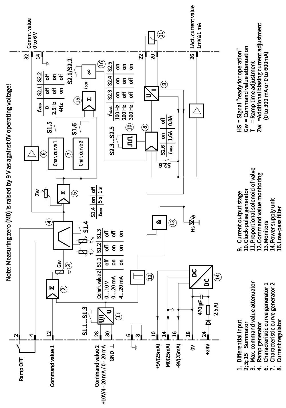
The command value voltage is applied to command value input 1 either directly or via an external command value potentiometer with the help of the regulated +9V voltage from the power supply unit [14].
The following is valid for this input: +9V ≜ +100%
External command value feedforward:
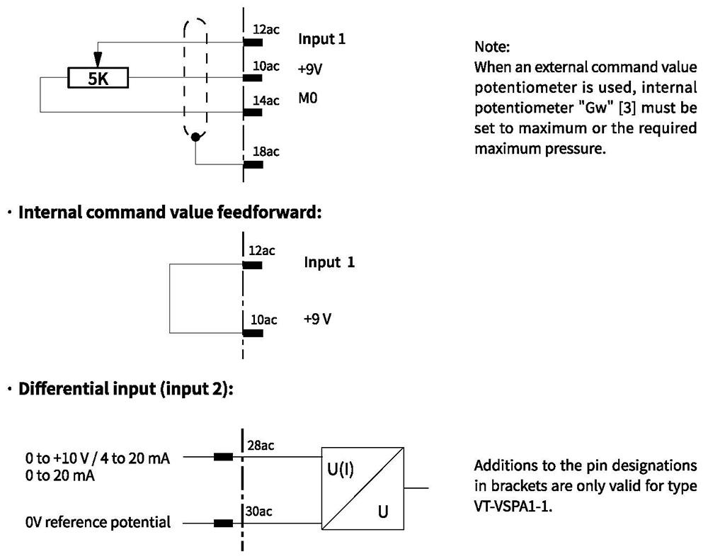
Command value input 2 is a differential input [1] (0 to + 10V). With the help of DIL switches ²⁾ it can be configured as current input (4 to 20mA or 0 to +20mA). If the command value is fed forward by external electronics with a different reference potential (e.g. by a PLC), this input must be used. When the command value voltage is applied or withdrawn, care must be taken that both signal cables are disconnected from or connected to the input.
Before being passed on, both command values are summated [2] and then fed to a potentiometer [3] that is accessible on the front panel and acts as attenuator and limits the maximum command value.
The downstream ramp generator [4] generates a ramp-shaped output signal from a stepped input signal. The time constant of this signal can be adjusted separately for "up" and "down" ramps with the help of two potentiometers. The specified ramp time refers to a command value step-change of 100% and can be approx. 1s or 5s, depending on the setting of a DIL switch ²⁾. If a command value step-change of less than 100% is fed to the input of the ramp generator or when attenuator [3] is effective, the ramp time shortens accordingly.
Function and configuration
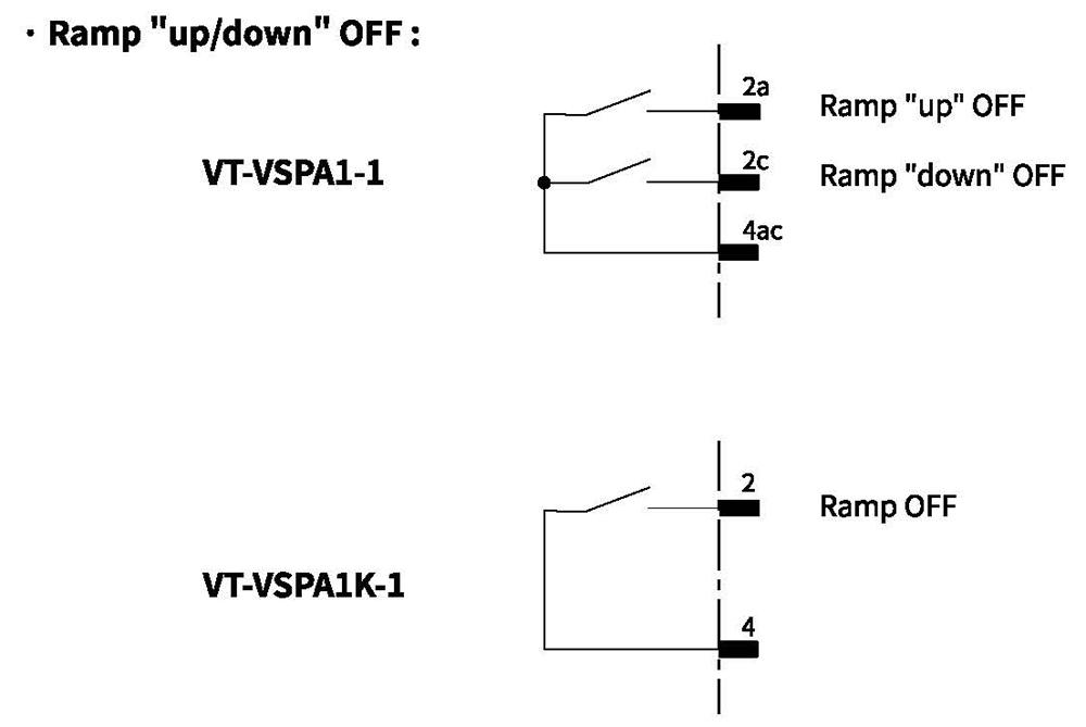
The following is valid for type VT-VSPA1-1:
The up and down ramp times can be set separately to their minimum value (ap-prox. 30ms) with the help of the external contacts "ramp up/down OFF".
The following is valid for type VT-VSPA1K-1:
The up and down ramp times can be set collectively to their minimum value (ap-prox. 30ms) with the help of the external contact
The output signal of ramp generator [4] is fed as current command value to the summing amplifier [5].
Here, a command value of 100 % corresponds to a voltage of +6V.
Summing amplifier [15] adds the output signals of the characteristic curve generators [6 or 7] to the command value (can be selected by means of DIL switches depending on the valve to be controlled). The current command value can alsvo be filtered through a lowpass filter that can be cut in.
Current out-put stage [9] is controlled via current regulator[8]. In addition, the current regulator modulates the current command value with clock-pulse encoder signal [10] (the frequency can be programmed with the help of DIL switches.
The clocked actual current value acts in the solenoid of the valve like a constant current with overlaid dither signal. Type VT-VSPA1-1 is provided with measuring sockets for the internal command value and the actual value.
The following is valid for the command value: +6V ≜ 100%
The following is valid for the actual value: 1mV ≜ 1mA
The signal "ready for operation" is output and LED "Hs"
on the front panel (with VSPA1-1) or LED "Hs" (with VSPA1K-1) is lit,
When:
– The solenoid cables are not short-circuited and the output stage is not overloaded,
– a command value is applied (cable break detection),
– there is no cable break present on the solenoid cable.
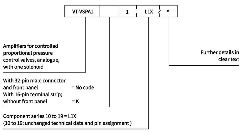
Ordering code
Block circuit diagram / pin assignment: VT-VSPA1-1
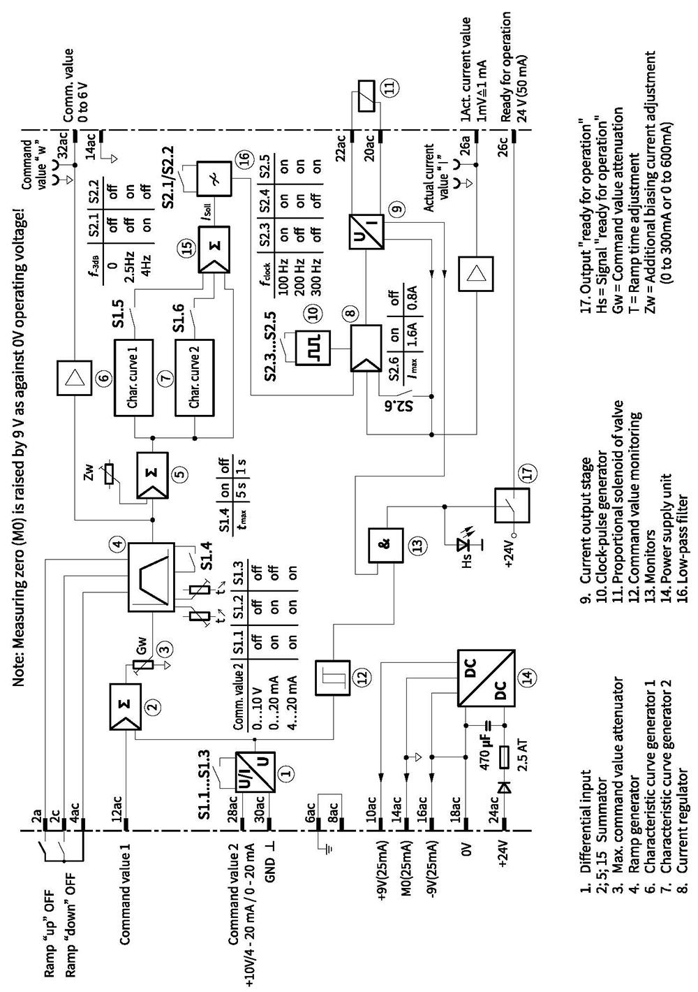
Block circuit diagram / pin assignment: VT-VSPA1K-1
Technical data
| Operating voltage Operating range: | - Upper limit value -Lower limit value | Uo Uo(t)max Uo(t)min | +24VDC+40%-5% +35 V +22V |
| Max. power consumption | Ps | <50 VA | |
| Max. current consumption | / | <1.8A L | |
| Fuse | FF | 2.5 AT | |
| Inputs: | -Command value 1 -Command value 2 (differential input) or or | U1 Ui 4 4 | 0 to+9 V (reference potential is MO) 0 to+10V; Re=100KΩ 4 to 20 mA (load Rg=100Ω) depending on setting with S11 to S13 0to 20 mA (load RB=100Ω) |
| Ramp time (adjustment range) | t | 30 ms to approx. 1s or 5s (depending on setting with S14) | |
| Outputs: | -Output stage ·Solenoid current/resistance or ·Biasing current at / max=800mA at /max=1600mA additionally at max=800mA at/max =1600mA ·Clock frequency | Imax max 1v 1v 1v 1v f | 800mA+20%, R20=19.5Ω depending on setting 1600mA+20%, R20=5.4Ω with S26 50mA or 100mA depending on setting 100mA with S26"and "Zw" 0 to 300mA+20% Adjustable by means of "Zw" on the 0 to 600mA+20% printed-circuit board 100Hz,200Hz,300Hz or 370Hz±10%each (depending on setting with S23 to S25) |
| - Signal "ready for operation" (only with VT-SPA1-1) ·Rready for operation ·Break down | U U | approx.Uo,50mA Load resistance>10kΩ OV,Ri=10kΩ | |
| - Regulated voltage | U | ±9V±1%, ±25 mA externally laodable | |
| - Measuring sockets ·Command value "w" ·Actual current value "I" | U U | 0to +6V (+6V 스 100% solenoid current), Ri=1kΩ 0 to 1600mV 스 0 to 1600mA ±20mA | |
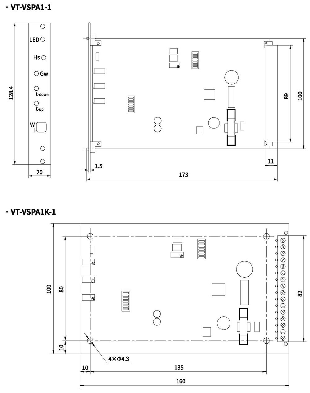
| Type of connection | - VT-VSPA1-1 -VT-VSPA1K-1 | 32-pin male connector, DIN 41612, form D 16-pin terminal strip | |
| Card dimensions: | Euro-card 100x160 mm, DIN 41494 | ||
| Front panel dimensions | -Height - Width soldering side -Width component side | 3HE(128.4mm) 1TE(5.08mm) 3TE | |
| Permissible operating temperature range | 9 | 0 to+50℃ | |
| Storage temperature range | 9 | -25to+85℃ | |
| Weight | m | 0.1kg | |
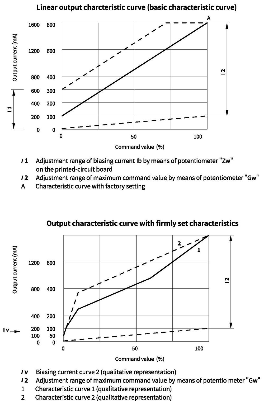
4 The maximum current /max can be set to the required value by means of command value attenuator potentionmeter "Gw".
Output characteristic curves
Indicator/adjustment elements

Indicator / adjustment elements
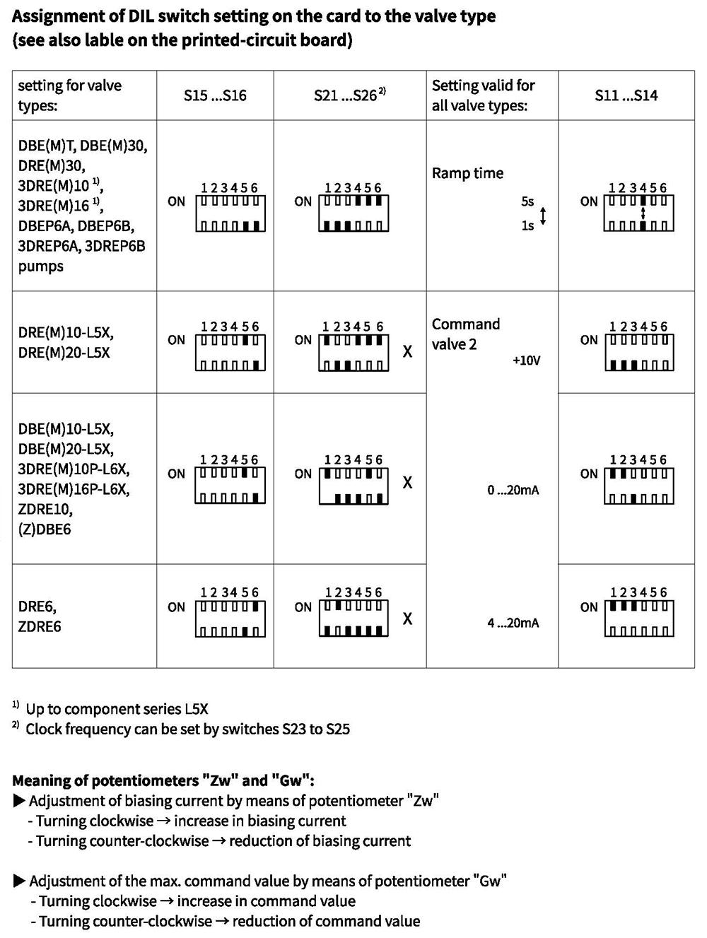
Meaning of the DIL switches
Note (X): Before commissioning the amplifiers, make sure that the DIL switches on the printed-circuit board are set according to the relevant application.
Switch positions with reference to the current valve types or previous amplifier cards
| DIL Switch | Valve types/amplifier cards | |||
| DBE(M)T, DBE(M)30 DRE(M)30,3DRE(M)10 3DRE(M)16 DBEP6A, DBEP6B 3DREP6A,3DREP6B pumps | DRE(M)10-L5X DRE(M)20-L5X | DBE(M)10-L5X DBE(M)20-L5X ZDRE10 (Z)DBE6 3DRE(M)10P-L6X 3DRE(M)16P-L6X | DRE,ZDRE6 | |
| VT 2000 | ||||
| S15 S16 | Characterist | ic curves | ||
| Basic characteristic curve OFF OFF | Characteristic curve 1 ON OFF | Characteristic curve 1 ON OFF | Characteristic curve 2 OFF ON | |
| S21 S22 | Command value filters | |||
| OFF OFF | f-3dB=4Hz ON OFF | f.3dB=4Hz ON OFF ) | f-3dB=2.5Hz OFF ON | |
| S26 | Max.output current 1 | |||
| Imax=800mA ON | Imax=800mA ON | max=1.6A OFF | /max=1.6A OFF | |
| S23 S24 S25 | Clock freq | uency | ||
| f=200Hz OFF ON ON | f=200Hz OFF ON ON | f=300Hz OFF OFF ON | f=370Hz OFF OFF OFF | |
| "Zw" | Basic biasing current setting | |||
| 100mA | 50mA | 100mA | 100mA | |
¹) Doubling of the maximum output current doubles the adjustment range and the set biasing current.
Adjustment range of biasing current using potentiometer "Zw"
I_max = 800mA → I_v = 0 to 300mA
I_max = 1600mA → I_v = 0 to 600mA
Adjustment options inedependent of the valve type (command value 2 and ramp time)
| S11 S12 S13 | Configuration of differential input | ||
| Command value 2:+10V OFF OFF OFF | Command value 2: 0 to 20mA ON ON OFF | Command value 2: 4 to 20mA ON ON ON | |
| S14 | Max. ramp time | ||
| OFF 스 1S | ON 스 5S | ||
Note: Factory setting (corresponds to the configuration lf a VT 2000 amplifier).
Unit dimensions